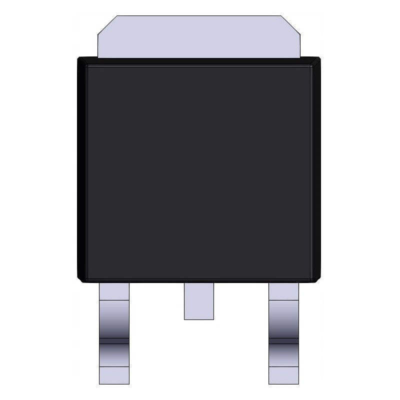
AOD403 D403 tranzystor MOSFET P-kanałowy 30V 70A TO252
  • AOD403 D403 tranzystor MOSFET P-kanałowy 30V 70A TO252
  • AOD403 D403 tranzystor MOSFET P-kanałowy 30V 70A TO252
  • AOD403 D403 tranzystor MOSFET P-kanałowy 30V 70A TO252

AOD403 D403 tranzystor MOSFET P-kanałowy 30V 70A TO252

€0.87
VAT included delivery in Poland 1-2 dni InPost

Volume discounts

Quantity Unit price You Save
20 €0.86 €0.17
40 €0.85 €0.69
60 €0.84 €1.56
100 €0.82 €4.33
Quantity
Available in Polish warehouse

Place an order within 12h 44m 44s And we will send your order today
help_outlineAsk about product
AOD403 D403 tranzystor MOSFET P-kanałowy 30V 70A TO252

AOD403 D403 tranzystor MOSFET P-kanałowy 30V 70A TO252

I accept privacy policy rules  

AOD403 tranzystor MOSFET P-kanałowy

  • Model AOD403
  • Oznaczenie D403
  • Typ MOSFET P-kanałowy
  • Maksymalne napięcie dren–źródło VDS = -30 V
  • Ciągły prąd drenu ID = -70 A (Tc = 25 °C)
  • Niska rezystancja w stanie przewodzenia
  • RDS(on) < 6,2 mΩ @ VGS = -20 V, ID = -20 A
  • RDS(on) < 8 mΩ @ VGS = -10 V, ID = -20 A
  • Niski ładunek bramki i niska rezystancja bramki

Parametry elektryczne:

  • Napięcie progowe bramki VGS(th): -1,5 do -3,5 V (typ. -2,5 V)
  • Maksymalne napięcie bramka–źródło VGS = ±25 V
  • Całkowity ładunek bramki Qg: typ. 51 nC, maks. 61 nC
  • Ładunek bramka–źródło Qgs: typ. 12 nC
  • Ładunek bramka–dren Qgd: typ. 16 nC
  • Transkonduktancja gFS: typ. 42 S
  • Rezystancja bramki Rg: typ. 3,8 Ω
  • Maksymalna energia lawinowa EAS = 125 mJ (L = 0,1 mH)
  • Maksymalna moc strat PD = 90 W (Tc = 25 °C)
  • Impulsowy prąd drenu IDM = -200 A
  • Temperatura złącza i przechowywania: -55 °C do +175 °C

Parametry dynamiczne:

  • Pojemność wejściowa Ciss: typ. 2890 pF
  • Pojemność wyjściowa Coss: typ. 585 pF
  • Pojemność zwrotna Crss: typ. 470 pF
  • Czas opóźnienia załączenia td(on): typ. 16 ns
  • Czas narastania tr: typ. 12 ns
  • Czas opóźnienia wyłączenia td(off): typ. 45 ns
  • Czas opadania tf: typ. 22 ns

Wbudowana dioda:

  • Maksymalny ciągły prąd diody IS = -70 A
  • Napięcie przewodzenia diody VSD: typ. -0,7 V, maks. -1,0 V
  • Czas odzyskiwania zdolności zaporowej trr: typ. 18 ns, maks. 22 ns
  • Ładunek odzyskiwania Qrr: typ. 11 nC, maks. 13 nC

Obudowa i montaż:

  • Obudowa TO-252 (DPAK)
  • Przeznaczony do montażu powierzchniowego (SMD)
  • Maksymalna rezystancja termiczna złącze–obudowa RθJC = 1,6 °C/W
  • Maksymalna rezystancja termiczna złącze–otoczenie RθJA = 50 °C/W

Zastosowania:

  • Układy przełączania dużych prądów
  • Układy sterowania i przełączania obciążeń
  • Przetwornice i układy zasilania
  • Aplikacje wymagające niskiej rezystancji RDS(on)
  • Układy wymagające wysokiej wydajności prądowej i dobrego odprowadzania ciepła

Odpowiedniki: UT70P03, HSU100P03, AOD423, VBZE100P03, HM70P03K, FDD9509L-F085, CMD170P03A, AP100P03D, ASDM30P100KQ

Zdjęcie przedstawia oferowany produkt. Czytelność zdjęcia została zwiększona za pomocą algorytmów AI.
Pomiar realny

K1421/A8(ID402238870)
95 Items
5905042152166

High Voltage and Current – This component can operate at high voltages and currents, posing a risk of electric shock. Pay attention to the maximum voltage and current values, as well as appropriate markings indicating these limits.

Caution During Installation – Ensure that the components are correctly mounted in the circuit, as improper connections can lead to overheating, damage, or fire.

Hot Components – Electronic components may heat up during operation, so it is important to follow the recommendations regarding the maximum operating temperature. Appropriate heat sinks or cooling systems should be used to ensure effective heat dissipation. Caution should also be exercised to avoid burns.

Swallowing Hazard – Small fastening components, such as screws, nuts, or washers, can pose a choking or swallowing hazard, especially for children. They should be stored in a place out of reach of children.

Spreading of Small Components – These components can pose a tripping or loss hazard during work. They should be stored in containers that prevent spillage.

Manufacturer (Private Label) (EU) 2023/988 (GPSR)
Name: Superelektronika sp. z o.o.
Address: ul. gen. K. Sosnkowskiego 26/83
05-300 Mińsk Mazowiecki, Poland
E-mail: sklep@superelektronika.pl
Responsible Person (EU) 2023/988 (GPSR)
Name: Superelektronika sp. z o.o.
Address: ul. gen. K. Sosnkowskiego 26/83
05-300 Mińsk Mazowiecki, Poland
E-mail: sklep@superelektronika.pl

You might also like

Comments (0)
No customer reviews for the moment.