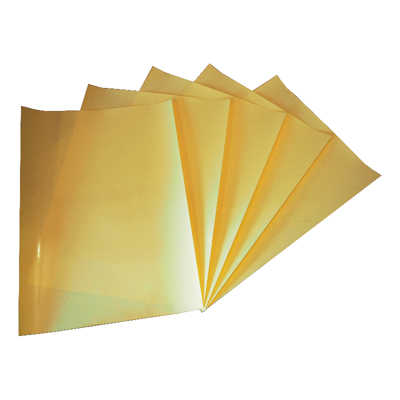
The thermal transfer paper is specially designed for transferring printed circuit tracks (PCBs) onto copper laminate using the thermal transfer method. It is designed for use with laser printers only and works by pressing the toner into the copper surface.
Technical data :
Quantity 5 sheets
Paper size: A4 (210mm x 297mm)
Weight: 188 g/m²
Colour yellow
Use for laser printer
The paper has a matt and a glossy side.
The fleece side is used for printing.
Quick guide to using thermal transfer paper:
1. Print pattern
Print the PCB with a laser printer on the fleece side of the paper.
Mirror the design for the bottom layer (Bottom Layer).
2 Transfer pattern
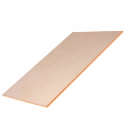
Clean the copper laminate (sand and degrease).
Lay the print with the toner facing the copper.
Press with an iron (max temp, no steam) for 3-5 min or use a laminator.
Cool and immerse in water until paper dissolves.
3. etching of PCB
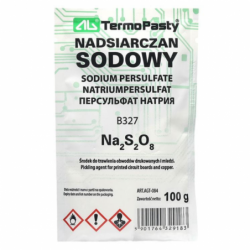
Dip in ferric chloride (FeCl₃) or B327 until the copper is etched (~10 min).
Rinse with water and wash off the toner with acetone.
4 Finish
Drill holes, optionally coat paths with tin or rosin.
Warnings !!!
This product is intended for persons with experience in electronics and chemical processing.
Danger of burns - caution required when using iron or laminator.
Contact with chemicals hazardous to health - ferric chloride (FeCl₃) and B327 are corrosive, require gloves and protective goggles.
Risk of vapour poisoning - PCB etching and cleaning should take place in a well-ventilated room.
Obligation to dispose of chemical waste properly - used solutions must not be poured down the drain.
Product for professional use - inappropriate use may lead to damage to equipment or health hazards.
We offer PCB copper laminates and sodium persulphate B327
K1177/MAGAZYN(ID324089749)
70 Items
5905427018858
Manufacturer (Private Label) (EU) 2023/988 (GPSR)
Name:
Superelektronika sp. z o.o.
Address:
ul. gen. K. Sosnkowskiego 26/83 05-300 Mińsk Mazowiecki, Poland